call now
+65-6391 9891
PCB design service and turnkey electronic engineering solutions
PCB Design Services
Evonix has the tools and knowledge to design your PCB no matter how large or small. We use the industries top tier design tools and are driven to be the best.
- HDI Designs with micro vias and advanced materials - Via-in-Pad, laser micro vias
- High speed, multi layer digital PCB designs - Bus routing, differential pairs, matched lengths.
- PCB Designs for space, military, medical and commercial applications
- Extensive RF and analog design experience (printed antennas, guard rings , RF shields...)
- Signal integrity issues to meet your digital design needs (tuned traces, diff pairs...)
- PCB Layer management for signal integrity and impedance control
- DDR, DDR2, DDR3, SAS and differential pair routing expertise
- High density SMT designs (BGA, uBGA, PCI, PCIE, CPCI...)
- Flex PCB designs of all types
- Low level analog PCB designs for metering
- Complete assembly drawings
- In-Circuit Test data generation (ICT)
- Drill, panel and cutout drawings designed
- Professional fabrication documents created
- Autorouting for dense PCB designs
Electronic Engineering Services & Complete Product Development
Complete Product Development Services
Evonix can provide a complete turnkey engineering and manufacturing solution. No matter what your quantities, we can produce everything you need and deliver a fully funtioning product right to your door.
- All types of electronic hardware design;
- Reverse Engineering
- Analog, digital and RF
- Schematic capture
- PCB Design
- BOM creation
- Firmware development
- Prototype building
- Full turnkey production of finished product
Electronic Engineering and Design Services
No matter how complex your idea, we can design it! From DSP's to FPGA's to RF communications Evonix PCB Design can do it all. Contact us today to see how we can help you.
- Full turnkey electronic engineering for space, military, commercial and consumer applications
- RF circuit design for communications
- PCB Antenna design
- Analog circuit design
- Digital circuit design
- Firmware development - Embedded
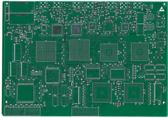
PCB Manufacturing
Send us your gerber files and we can have your PCB made with the best quality at an affordable price.
Standard Capabilities:
| Materials FR-4 Fr-5 FR406 FR408 Nelco Buried Capacitance Polyimide Teflon Rogers Taconic Arlon Hybrid FR-4 / Rogers |
Layer Count: 1 to 24 Layers |
| Minimum line spacing: 0.003" |
0.003" 0.002" to 0.200" |
| Minimum Annular Ring: 0.005" |
Minimum drilled hole size: 0.008" |
| Maximum board size: 35" x 46" |
Maximum Copper Thickness: 5oz. |
| Solder Mask: SMOBC, LPI or Dry Film |
Finish Plating: HASL Lead Free HASL Immersion Silver ENIG Matte Tin Plate Soft / Hard Gold for Tabs and SMT Selective Gold Palladium |
| Silkscreen Colors: White Yellow Black |
Solder Mask Colors: Green Blue Red Black Clear |
| Panelization: Routing V-Groove |
Other Services: Plated Slots Edge Plating Controlled Dielectrics Tented Vias Conductive Filled Vias Blind/Buried Vias ITAR |


Singapore Address
10,Jalan Besar,
#B1-15 Sim Lim Tower,
Singapore-208787.
Tel:+65-6391 9891
India Address
42,Thiruvalluvar Street,
Nehru Nagar,
Saligramam,
Chennai-600093.
Site Designed By s.udhayasuriyan@webesolutions.in

