call now
+65-6391 9891
PCB design service and turnkey electronic engineering solutions
PCB Design Flow
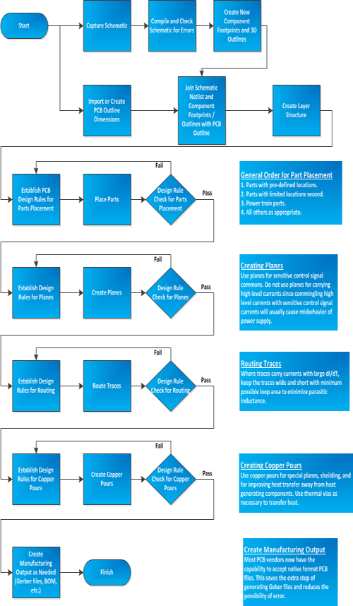
Our PCB designers are all trained to perform 100% manual placement and routing of your board. We will constantly review the design with customer to obtain approval.
In post-process, we generate all necessary Gerber manufacturing files, and perform Gerber review and check among our PCB designer internally. The reliability of the Gerber data greatly reduces front-end queries from the PCB manufacturer and allow faster turn-around time and reduced tooling costs.
With regular in-house design reviews and consultation with customers, we are able to provide the highest quality of PCB design to our customers’ requirement on time, every time.
Design Capabilities
- High Layer Count PCB
- Blind, Buried & Micro Via
- Mixed-Signal Design
- High-Power Circuit Design
- High-Speed Design
- High-Density Design
- Micro-BGA and BGA
- Matched Length Traces
- Controlled Impedance For Single Ended & Differential
- EMI/EMC Compliance
- Embedded Resistor
- HDI Technology
- COB
- Flex Design
- Rigid Flex Design
- MCM
- RF Design
Design Verification
- DFM & DFT
- IPC & Mil Standard
- EMC / EMI
- Hi-Speed rules
- Gerber checking using CAM tool
- In-process cross QC
Design Deliverables
- Fabrication Drawings
- Assembly Drawings
- Gerber Data
- Drill Data
- Design Database
- Customized Output Files
Design Tools / Skills
- Mentor Graphics - Board Station
- Mentor Graphics - PADS
- Altium Designer
- Cadence (Allegro)
- CAM 350 / Camtastic 2000
- PROTEL99SE
- Eagle
- Express PCB
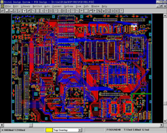
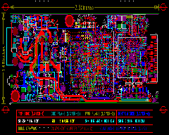
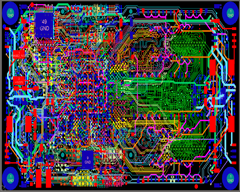
PCB Design Samples


Singapore Address
10,Jalan Besar,
#B1-15 Sim Lim Tower,
Singapore-208787.
Tel:+65-6391 9891
India Address
42,Thiruvalluvar Street,
Nehru Nagar,
Saligramam,
Chennai-600093.
Site Designed By s.udhayasuriyan@webesolutions.in

